Артемий Лебедев не прав: чем Силиконовая Долина лучше, чем Мытищи
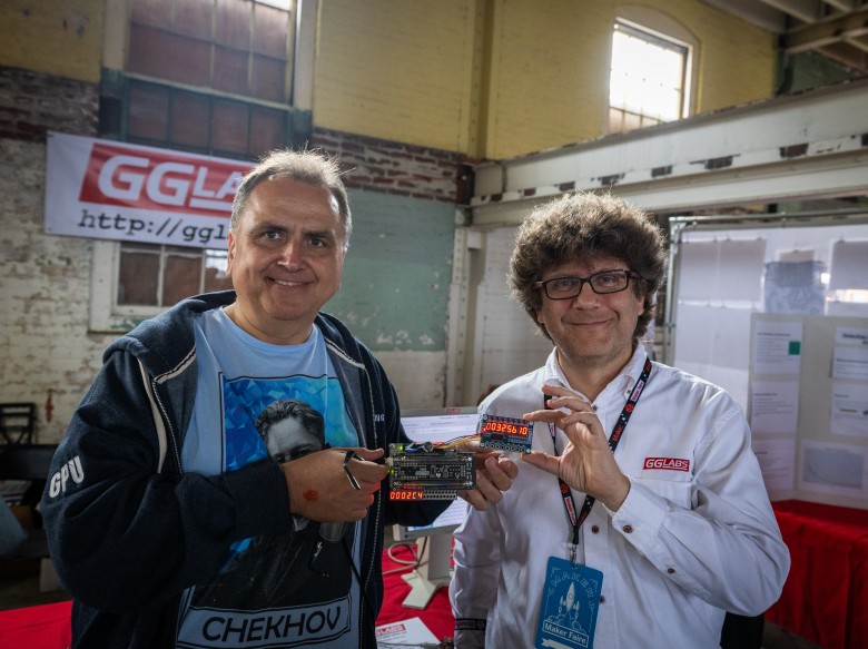
A Geiger-Müller radiation counter from GGLabs connected to Terasic DE10-Lite board with Altera MAX 10 FPGA
Артемий Лебедев недавно сделал стрим, в котором утверждал, что Силиконовая Долина хуже, чем Мытищи. При том, что я согласен с Лебедевым, что например музей искусств в Сан-Хосе не больше, чем картинная галерея в Мытищах, но есть область, в которой Силиконовая Долина кроет Мытищи, как бык овцу:
В Мытищах заведомо меньше, чем в Силиконовой Долине людей, которые понимают красоту микроархитектуры цифровых схем на уровне регистровых передач. Для Лебедева это пустой звук, так как он дизайнер шрифтов, лого и вебсайтов, а не CPU, GPU и сетевых чипов. Но среди работников Apple, NVidia, Samsung, Cisco, Intel и других местных компаний дизайнеров чипов заведомо больше, чем в Мытищах.
Эти позиции нужны и для проектирования айфонов, и для проектирования ракет:

При этом я не стану говорить, что Мытищи - некультурный город. Напротив, там есть машиностроительный и приборостроительный заводы, конструкторские бюро которых некомненно используют уже готовые встроенные микропроцессоры, ЦОС и ПЛИСы. Однако если в Мытищах и есть дизайнеры самих чипов, то бишь ASIC-ов, то они скорее всего ездят в Зеленоград или работают удаленно.
О чем вообще идет речь? Не о программировании (про то, что в Мытищах есть компетентные программисты, я не спорю).
Ниже моя заметка про наше с коллегой из SiFive мероприятие в Маунтин-Вью, Калифорния в воскресенье. На мероприятии программисты могут увидеть и даже поучаствовать в проектировании микросхем на уровне регистровых передач, с помощью синтеза на языках описания аппаратуры. Я притащу туда больше дюжины компьютеров с предустановленным софтвером для синтеза и более 30 FPGA плат. Если вы в Силиконовой Долине - заходите (а то Лебедев говорит «в Силиконовой Долине некуда ходить»), а если нет - то можете почитать для общего развития, если вы еще не знакомы с этой темой.
На митапе будет девушка Маша, она работает инженеркой в компании Broadcom и обещала прийти на мероприятие:

Итак:
Why would a software engineer attend an FPGA hardware meetup at Hacker Dojo?
For the last 30 years digital chip design is not done by schematic entry anymore: hardware engineers write code just like software engineers.
The difference is that the code a software engineer writes becomes a chain of CPU instructions stored in memory, while the code a hardware engineer writes in a hardware description language (HDL) becomes the CPU itself, its transistors and metal connections. And not only CPU: the same technique is used to design processor-less ("fixed function") blocks in GPU that shuffle triangles and pixels, as well as network router chips that edit packet headers 100 times faster than CPU.
There are ways to experience this workflow without paying a million dollars to a silicon fab. One way is simulation, and another way is to use a matrix of reconfigurable logic cells, a Field Programmable Gate Array (FPGA). You can come on January 14 to Hacker Dojo in Mountain View, California. We have a bunch of computers and FPGA boards, and we will show you how to use them not only to blink LEDs but also to output graphics and recognize music.
This will change your perspective of what the code is. Some details:

The room we booked in Hacker Dojo for the meetup
At the meetup, we are going to have a dozen computers, with both Linux and Windows, as well as the preinstalled design and simulation software, everything with free license or open-source:
- Intel Quartus Prime Lite 23.1
- Altera Quartus II Web Edition 13.0sp1 for older boards
- AMD Xilinx Vivado ML Standard Edition 2023.2
- Gowin V1.9.9Beta-4 Education
- Gowin Programmer V1.9.9 Beta-4 Education
- openFPGALoader
- Icarus Verilog v12.0
- GTKWave
- Open Lane
You can use one of these computers, or you can bring your own computer and install the software by yourself, or we can give you a bootable SSD you can plug into your computer and work with the pre-installed environment. I made a photo of an SSD on piano because some of our exercises do music recognition:

We are going to explain everything from ground zero at the meetup, but you can also read some theory below. First, let's compare the workflow in software programming and in hardware design.

The flow in hardware design is called RTL-to-GDSII. RTL means "Register Transfer Level", an abstraction model used when writing the code in a Hardware Description Language (HDL) such as Verilog / SystemVerilog or VHDL. GDSII is a file format representing geometric shapes, a blueprint of a chip sent to a silicon fab to manufacture this chip.

The vast majority of the devices that do any information processing today combine silicon designed using compilation (synthesis) from hardware description languages and software created using compilation from software languages:

ASIC is an acronym for Application-Specific Integrated Circuit. An example of an ASIC is a chip that runs Android or iOS on your smartphone. Another example is a chip that edits and forwards packets in a core router. Or practically any modern big chip (back in 1980, there was a distinction between full-custom and ASIC, but it is not meaningful anymore).
SoC, System on Chip, is an ASIC that has one or several processor cores, memories and other components, such as GPU or DSP, that form the whole computer system on a single chip
Controllers of the peripheral devices are also created using HDLs. As well as GPUs, ML accelerators, and fast packet processing in networking chips:

How can we create such hardware without a silicon foundry (a fab)? Using a synthesis flow for FPGA. It starts from the same code in SystemVerilog but ends up not in a GDSII file, but in a so-called bit file, which is loaded into a configuration memory of FPGA.

FPGA is a matrix of cells that contain so-called LUTs, LookUp Tables, and D-Flip-Flops, the minimal state/memory devices. The simplest version of a D-flip-flop can store 1 bit of data during 1 clock cycle.

Lookup Table (LUT) is a clever idea that allows to form any logic function of two inputs y = f (x0, x1) - by defining four bits (a, b, c, d) stored in a configuration memory of FPGA. We can think of { x1, x0 } as a 2-bit address for a 1-bit wide 4-bit deep memory with a content { a, b, c, d }.
In other words f (0, 0) = a; f (0, 1) = b; f (1, 0) = c; f (1, 1) = d. If we define abcd=0001, f becomes AND logic gate, if we define abcd=0111, it becomes OR logic gate and so on.
The LUT can be implemented using three multiplexers, or muxes. Each mux is a hardware equivalent of a software "if" statement, a mechanism for making a choice:

Once we add to the picture D-flip-flops, the primitives for storing state, we can build hardware with complicated behavior in time, such as finite state machines and CPU pipelines.
We can create a design that counts a particle of radiation:
Another our example uses FPGA to recognize music (no software involved, just a digital circuit implemented in reconfigurable hardware):
We can also generate computer graphics by creating combinational logic that implements a function RGB=f (X, Y), where RGB are the values of red, green and blue color channels, and X and Y are pixel coordinates. When this combinational logic is connected to a VGA controller, we can output some pictures on a monitor connected to the FPGA board. This is a great way to practice logic design in SystemVerilog:

SiPEED Tang Primer 20K Dock FPGA board connected to TM1638-based peripheral board and a graphic display
You can add some counters and FSMs and create a computer game with moving sprites.
Or you can build your own RISC-V CPU:

What would you do with this knowledge? Some people can consider starting a career in digital design and verification of ASIC or FPGA. Others can use this skill to design heterogeneous systems that include software and off-the-shelf hardware together with custom hardware accelerators - this is especially important in AI/ML.
The event is not only for the beginners. Since our Portable SystemVerilog Examples for ASIC and FPGA initiative aims to create a vendor-neutral multi-toolchain multi-FPGA-board set of examples, some seasoned professionals can use it as an opportunity to explore a new toolchain: Altera, Xilinx, GoWin, Lattice or Yosys (which compatible with some Lattice and GoWin parts. Right now we support more than 30 FPGA boards and even more variations with peripherals:

The current support for IntelFPGA / Altera boards is pretty good: we support many inexpensive boards from Terasic: DE0, DE0-CV, DE0-Nano, DE10-Lite, DE10-Nano, DE1-SoC, DE2-115, Cyclone V GX Starter Kit.
We also support many non-Terasic boards with Altera FPGA found on AliExpress: Saylinx, Omdazz/RzRd, EPI-MiniCY4 from emooc.cc as well as older boards ALINX AX4010, Piswords-06 and Zeowaa. Some older boards are still used in universities all over the world.
The rest of the Altera boards are mostly either expensive (i.e. not suitable for student use) or rare. Nevertheless, there are several Altera boards on our TODO list, and adding support for them is a relatively easy exercise for a new member who wants to join the initiative.

The list for Xilinx support is smaller, but we cover many popular boards: Arty A7, Basys3, Nexys4, Nexys4-DDR / Nexys A7 and Zybo Z7.
We intentionally do not support Xilinx Spartan-6 and Spartan-3 because these older FPGAs require an older EDA toolchain called ISE, which does not support SystemVerilog, only Verilog-2001. We support only FPGAs supported by the current version of Xilinx Vivado ML Standard Edition. Vivado does support SystemVerilog standard to a reasonable level.

The boards in the TODO list, but not covered yet include Zynq (in progress) and some breadboardables: Cmod S7 with Spartan 7 (a.k.a. PLTW S7 - an interesting educational project to expose high school teenagers to digital logic design) and Cmod A7 with Artix-7. An interesting feature of Cmod S7 - it has true off-chip SRAM, not SDRAM like many other boards:

Out Gowin list includes support for Tang Primer 20K Dock, Tang Nano 20K and Tang Nano 9K. We are compatible with the Gowin EDA toolchain and Yosys-based open-source toolchain (in progress). We are using openFPGALoader to configure Gowin FPGAs under Linux and the commercial Gowin programmer (educational edition) under Windows. There are several boards on the TODO list, but we have a good handle on them:

Lattice boards are a challenge. We do have many of them, but only 2 are supported, both only with Yosys-based toolchain and the person who did Lattice port cannot continue with the project, so this looks like a new area for the new participants:

Yosys-based ports for Gowin and Lattice are linked to another area of work: making all our examples compatible with open-source ASIC design tools, primarily Open Lane.

Compatibility with Open Lane is strategically very important because it allows researchers and small startup companies to design and manufacture experimental ASICs for free or at a low cost of < $10K. This sounds impossible, given the typical ASIC project involves many millions of dollars, both in EDA tools and fixed manufacturing expenses. The catch is:
- The project might be sponsored by Google if they like what you design.
- The technology node is conservative - 130 nm.
- Open Lane is still an early product when evaluated against the commercial design tools from Synopsys and Cadence. Think of Linux versus Windows back in ~1993.
However, this option is still amazing because:
- 130 nm is still a decent technology for microcontroller design, and modern microcontrollers incorporate even hardware AI acceleration for IoT on edge.
- A researcher can create a proof of concept for a commercial ASIC without using funds from VCs or similar sources.
- The students can learn the intricacies of ASIC timing using such Open Lane - based projects, which is different from static timing analysis in FPGAs.
Here is a recent screenshot with the latest open designs from Google / Skywater / Efabless website:

We will cover all these topics (and more) during our meetup at Hacker Dojo. Join at LinkedIn and meetup.com. See you there!

The related posts about the event:
- The first Silicon Valley meetup on portable SystemVerilog examples for ASIC and FPGA
- Toward the January meetup on portable SystemVerilog examples in Silicon Valley
For those who want to proceed further after the event, some book recommendations:
- Digital Design and Computer Architecture, RISC-V Edition by Sarah Harris and David Harris
- Digital Design: A Systems Approach Illustrated Edition by William James Dally and R. Curtis Harting
- Logic Design and Verification Using SystemVerilog (Revised, 2016) by Donald Thomas
