PoE termination board
For my next big project I'm planning on making it run using power over ethernet. Back in March I designed a quick circuit using the TI TPS2376-H PoE termination chip, and an LMR16020 switching regulator to drop the ~48v coming in down to 5v. There's also a second stage low-noise linear regulator (ST LDL1117S33R) to further drop it down to 3.3v, but as it turns out the main chip I'm using does its own 5->3.3v conversion already.
Because I was lazy, and the pricing was reasonable I got these boards manufactured by pcb.ng who I'd used for the USB-C termination boards I did a while back.
Here's the board running a Raspberry Pi 3B+, as it turns out I got lucky and my board is set up for the same input as the 3B+ supplies.
One really big warning, this is a non-isolated supply, which, in general, is a bad idea for PoE. For my specific use case there'll be no exposed connectors or metal, so this should be safe, but if you want to use PoE in general I'd suggest using some of the isolated convertors that are available with integrated PoE termination.
For this series I'm going to try and also make some notes on the mistakes I've made with these boards to help others, for this board:
Coming soon will be a post about the GPS board, but I'm still testing bits of that board out, plus waiting for some missing parts (somehow not only did I fail to order 10k resistors, I didn't already have some in stock).
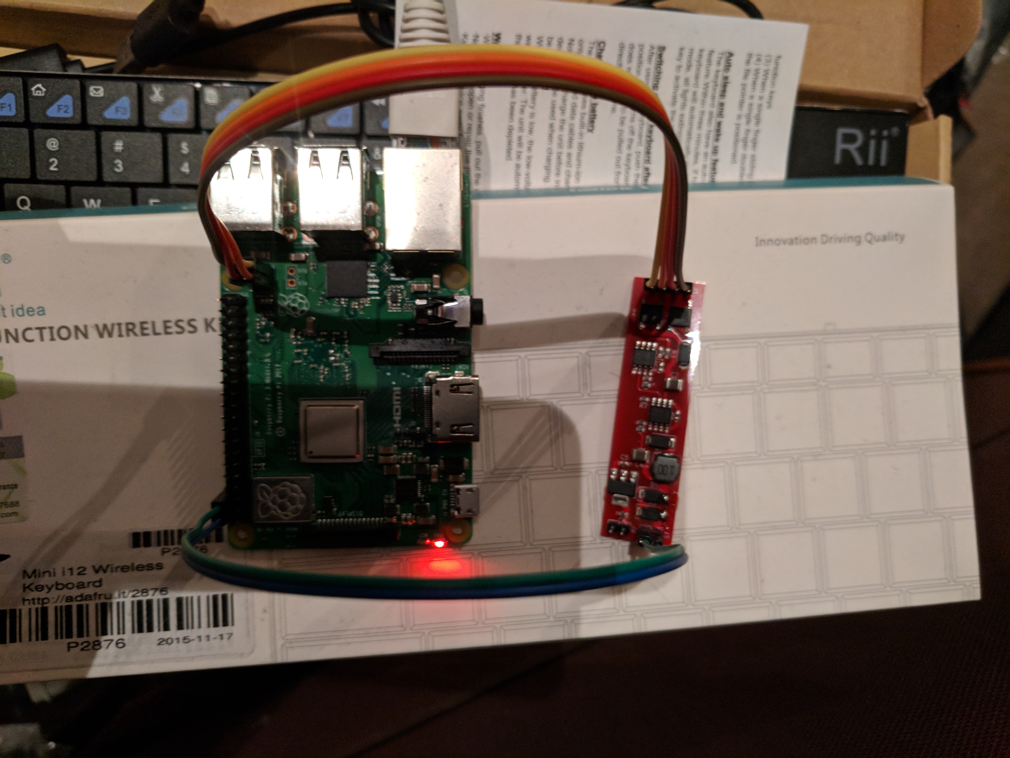
Because I was lazy, and the pricing was reasonable I got these boards manufactured by pcb.ng who I'd used for the USB-C termination boards I did a while back.
Here's the board running a Raspberry Pi 3B+, as it turns out I got lucky and my board is set up for the same input as the 3B+ supplies.
One really big warning, this is a non-isolated supply, which, in general, is a bad idea for PoE. For my specific use case there'll be no exposed connectors or metal, so this should be safe, but if you want to use PoE in general I'd suggest using some of the isolated convertors that are available with integrated PoE termination.
For this series I'm going to try and also make some notes on the mistakes I've made with these boards to help others, for this board:
- I failed to add any test pins, given this was the first try I really should have, being able to inject power just before the switching convertor was helpful while debugging, but I had to solder wires to the input cap to do that.
- Similarly, I should have had a 5v output pin, for now I've just been shorting the two diodes I had near the output which were intended to let me switch input power between two feeds.
- The last, and the only actual problem with the circuit was that when selecting which exact parts to use I optimised by choosing the same diode for both input protection & switching, however this was a mistake, as the switcher needed a Schottky diode, and one with better ratings in other ways than the input diode. With the incorrect diode the board actually worked fine under low loads, but would quickly go into thermal shutdown if asked to supply more than about 1W. With the diode swapped to a correctly rated one it now supplies 10W just fine.
- While debugging the previous I also noticed that the thermal pads on both main chips weren't well connected through. It seems the combination of via-in-thermal-pad (even tented), along with Kicad's normal reduction in paste in those large pads, plus my manufacturer's use of a fairly thin application of paste all contributed to this. Next time I'll probably avoid via-in-pad.
Coming soon will be a post about the GPS board, but I'm still testing bits of that board out, plus waiting for some missing parts (somehow not only did I fail to order 10k resistors, I didn't already have some in stock).